Description
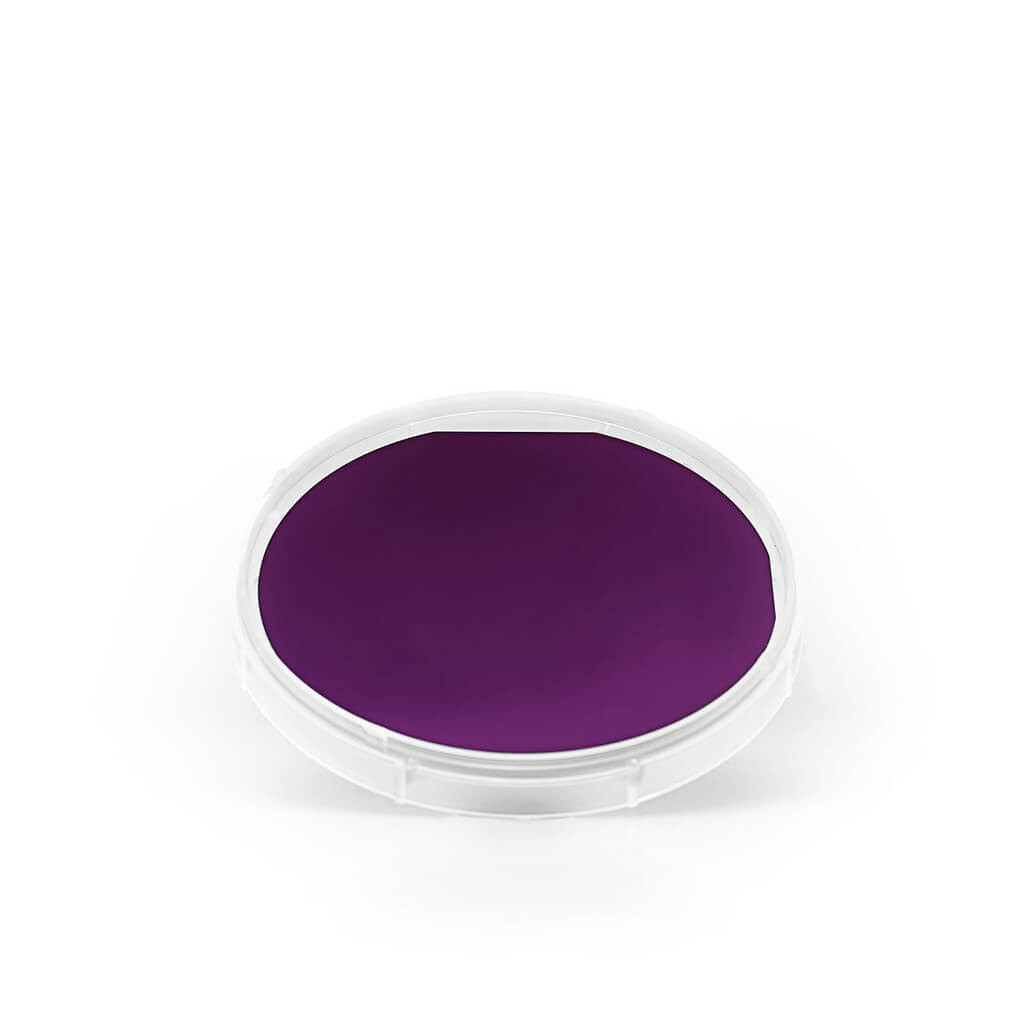
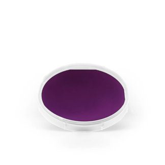
Monolayer Graphene Film on Si-SIO2 – 4″ round wafer
Our monolayer graphene on SiO2/Si (4” Wafer, fully covered) is a bi-dimensional material produced by CVD and transferred to a circular substrate of Si/SiO2 (300nm) by a wet transfer process. We consider it to be a benchmark product in the graphene market – not only for its excellent quality, but also for its shape, size and number of applications.
Graphene Film
Transparency: > 97%
Coverage: > 95%
Thickness (theoretical): 0.345 nm
FET Electron Mobility on Al2O3: 2000 cm2/Vs
FET Electron Mobility on SiO2/Si: 4000 cm2/Vs
Sheet Resistance: 580±50 Ohms/sq (1cm x 1cm)
Grain size: Up to 10 μm
Substrate SiO2/Si
Dry Oxide Thickness: 300 nm (+/-5%)
Type/Dopant: P/Bor
Orientation: <100>
Resistivity: <0.005 Ohm·cm
Thickness: 525 +/- 20 μm Front surface:
Single Side Polished Back Surface: Etched
Particles: <10@0.3 μm

